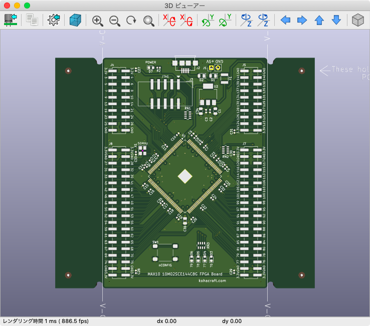
I previously designed an evaluation board and a stencil for a MAX 10 FPGA with many IO pins and ordered them to the SeeedStudio Fusion PCB.
I also received the MAX 10 FPGA I ordered to Maruz.

Now that I have everything, let's start assembling it.
Printing solder paste
Subtle relationship between the board and the stencil
In the past, when printing solder paste using a stencil, discarded boards with the same thickness were placed around the target board.

The stencil was fixed with tape.

At this time, the stencil position was finely adjusted to fit the stencil holes to the board land, and the stencil was fixed with tape.
The positioning is very severe when there is a narrow IC such as 0.5 mm.
Therefore, if you try to print more than one page, you may need to align the stencil each time.
Drill holes in the board and stencil

The main board is in the center, and there are discarded boards on both sides.
The main board and the disposable board can be separated by a V-cut.
Then, a hole of 1.0 mm in diameter is made in the upper and lower ends of the discard board.

There is a 0.9 mm hole in the same position as the hole on the disposable substrate.
The width of the thumbtack needle is 0.9 mm, so I tried making it that diameter.
(I used 0.9 mm, but I recommend 0.95 mm or 1.0 mm.)
Positioning procedure using pushpins
Then, let's actually position with pushpins.

A disposable substrate of the same thickness is placed in the front and back, and the target substrate is sandwiched, so that the central substrate does not move.
Fix the discarded board and the cardboard with tape.

Superpose the stencil on the board.

Insert a thumbtack into the stencil and the hole on the board.

No delicate alignment required.
Super easy.
Solder paste printing

Stir the solder paste well before placing it on the stencil.
The paste will be smooth, allowing for even printing.
You should stir it.

Place the solder paste on the far end of the stencil.

As you move toward the front at a speed of about 1 cm per second, the solder paste is printed on the board.

This is where the 0.5 mm pitch MAX 10 FPGA fits.
Solder paste is printed in perfect position.
I printed 3 of these boards, and they were all in perfect position.
Mounting electronic components

I mount electronic components. The IC with a large area cannot be picked with tweezers, so it can be easily placed with a vacuum pick.
Chip parts are placed on the board with Reverse operation tweezers.
With normal tweezers, when you pick up a part, too much force is applied and the part flies away.
Reverse operation tweezers will not cause such trouble at all.
I use SMD Reverse operation tweezers PT 28 made by engineers.
I don't want to do any more work with ordinary tweezers. Reverse operation tweezers are so convenient.
This time, we used a 1005 size component because we had to place many bypass capacitors around the FPGA.
The 1005 size is too small to be picked by the reverse operation tweezers of PT 28 above.
So, I bought a Reverse operation tweezers called P - 652 with a narrow end.
Now I can smoothly place the 1005 size part on the board.

The mounting is completed with the pin header of the surface mounting.
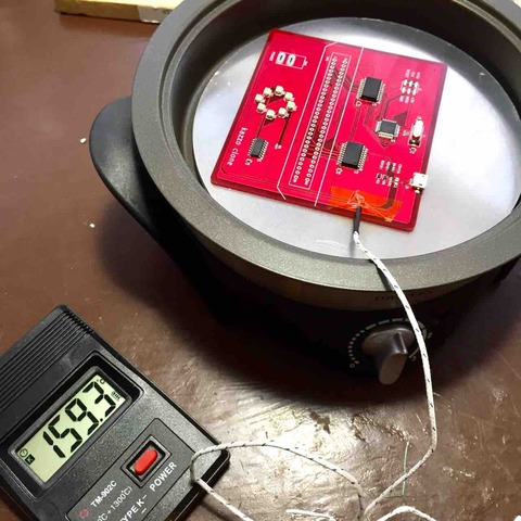
Reflow on a hot plate.

If you heat it while measuring the temperature of the board with a thermocouple, you can reflow it nicely without overheating.
This is what I use.
I only need to know the approximate temperature, so it's cheap enough.
Reflow complete

All you have to do is to cut off the discarded boards on both sides with V-cut grooves.
It was not a V-cut.

The place where I ordered V-cut is not V-cut!

I usually had a V-cut.
Next time, I will put it in the outline layer.

Use an acrylic cutter to dig grooves on both sides of the board.
But the board is hard and the blade is damaged immediately, so I can't dig deep.
Done!

The MAX 10 FPGA board was completed by separating the discarded board.

Since it is an all surface mounted part, there is no pin on the back side.
It does not short-circuit on the back of the board during the experiment.
This is convenient.
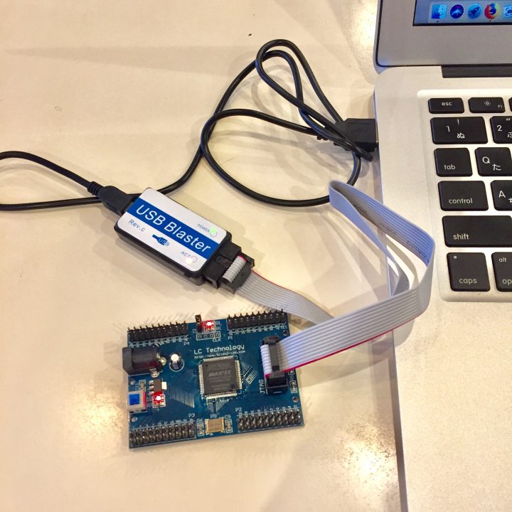
Will it be recognized by USB Blaster?

The Chinese USB Blaster clone cannot be set up gracefully with windows 10.
Here is the setup method.

I can see the 10M02 FPGA.
The FPGA was recognized successfully.
Turn on the LED

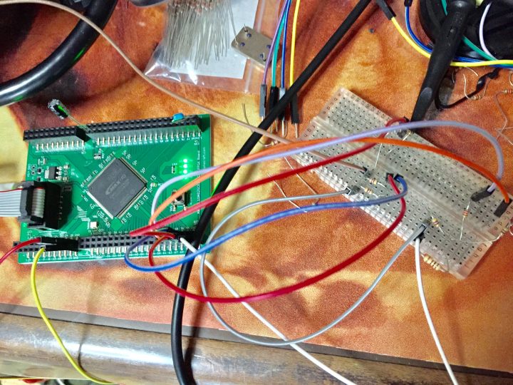
The board has a 50 MHz oscillator, so you can divide the clock and flash the LED.

FPAG also worked correctly.
This book is more detailed about how to use MAX 10.
I have this book, too.
The FPGA boards in this article are available here.


