Can I make a ROM writer?
What is a ROM writer?
Data is sent from a personal computer, converted into a ROM write signal, and written in an empty ROM.
What signals are required to write
Here is the data sheet for the STmicro UV-EPROM M27C256 that I bought with Aliexpress.
Power source type

Take a look at the instructions for writing a datasheet.

- Read Power : 5V
- Write Power : 12.75V and 6.25V
Write control method
Take a look at the diagram of the data sheet write waveform.

-
A0 - A14 : Addressing
-
Q0 - A7 : Data specification
-
Vpp : Signal to set to write mode (normally 5V, raised to 12.75V to set to write mode)
-
Vcc : Power supply (raised to 6.25V to set to write mode)
-
/ E (/ CS) : Write timing specification
-
/ G (/ OE) : Read timing specification
It is a fairly simple control method.
To summarize,
- set Vpp to 12.75V and Vcc to 6.25V to be in the write mode.
- specify the address and data
- If a low pulse is input to / E, it is written.
- When / G is set to Low, the written data is read, so check it.
I can do it with Arduino.
Making a ROM writer with Arduino
Is there enough IO pins?
The control method was not difficult, so I will consider making a lighter with an arduino which is a 5V microcomputer.
- addresses x 15
- data x 8
- Signals for setting Vpp and Vcc to the write mode x 1
- /E x1 , /G x1
The number of IO pins available to users of each arduino
- UNO : 18
- Leonardo : 21
- MEGA:46
UNO is not enough at all, MEGA is quite enough.The MEGA board is a little expensive, so I would like to think about the Leonardo board.I think I will use the Atmega32U4 that is used for Leonardo because it is expensive to buy Leonardo normally.
IO Pin Savings
It then converts the SPI signal into a 16 bit parallel signal.

The block diagram looks like the one above.
Only 3 "IO" can provide 15 ROM address wires.(Note : MOSI and IO in the figure were reversed)
Circuit design
ROM x 1

I added power control, control signals and data bus to the block diagram.(Note : MOSI and IO in the figure were reversed)Since the address bus is a shift register, the number of IO pins is considerably reduced.I need 14 pins in total.
The Atmega32U4 (Leonardo) still has a lot of pins, so I will be able to write to 2 ROMs.

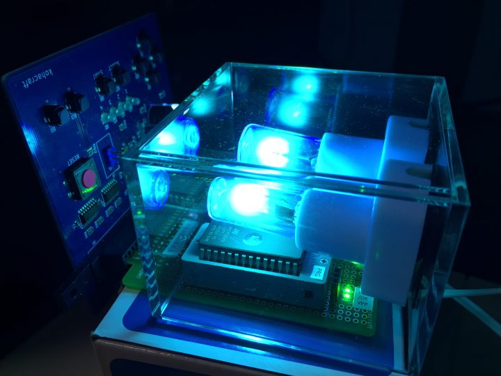
The right side of the picture above is the program ROM, and the left side is the character ROM. When making the ROM of the cassette of the Nintendo Famicom, it is necessary to write data in these 2 ROMs.
It is convenient if you can set 2 ROMs and write the program ROM and the character ROM together.
Expanded for 2 ROMs

This schematic has been extended to control 2 ROMs. I also assigned which IO pin to use. I think I can write to 2 ROMs with Atmega32U4 (Leonardo).
Power supply switching circuit
Consider a power supply and a circuit for switching the voltage. The power supply circuit uses an inexpensive DCDC module to produce 5V to 12.75V and 6.25V.
By adjusting the volume, the voltage can be raised to nearly 25V.
Using this DCCD, I think of a circuit like this.

When this is replaced with a circuit, it is like this ↓.

It is an OR circuit of the power supply using a diode.
The transistor can be anything as long as it is Nch, 2SC1815, etc.
Note that the diode at the end of the circuit causes a voltage drop.
Therefore, the voltage of the DCDC converter is not set to 6.25V or 12.75V, but adjusted so that the voltage after passing through the diode becomes 6.25V or 12.75V.
Mounted on the board
Start of soldering

I think I will go with this arrangement.

Next is the wiring behind the board.

Connect 5V to the pins here and there to check for incorrect wiring.
The power switch and circuit are working well.
It worked quite well.
Completion

I put a check LED on each address bus, data bus and control signal. The LED lights up to indicate which signal is ON, which is useful for debugging programming.
This board has a strange shape. It is designed to be inserted into my own microcontroller board.
Cassette Arduino

This is a micro controller board compatible with Arduino Leonardo which is currently being produced. It has a Famicom cassette slot that connects all the IO pins to the 32 bit parallel output. Insert the expansion board into this cassette slot to connect the HAT board to the Arduino. It is called "Cassette Arduino" and is currently under development.

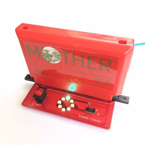
For example, if you insert a cassette like this ↓

That's good.
Therefore, the substrate we made this time is ↓

This is the ROM writer cassette. It's unprecedented that a ROM is stuck vertically, but it's interesting.
Now that the circuit is complete, I will program it. Will I be able to write well?
2019.6.21 Continuation Can now write to and read from ROM


