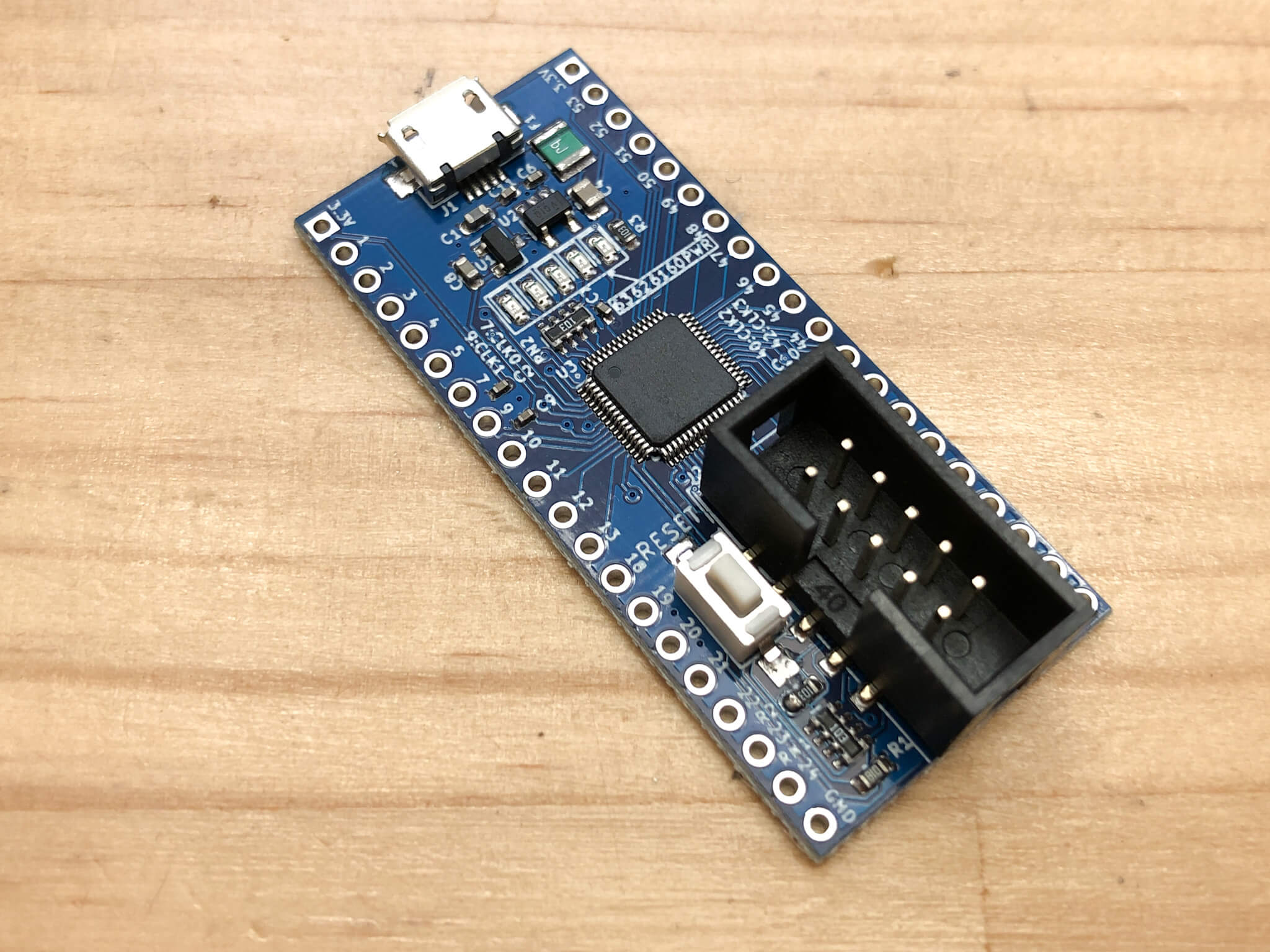
Previously, I made a MAX V 5M160 CPLD board that sticks into the breadboard.
After completion, I used it for a while and found it inconvenient. CPLDs are programmed to change state in sync with the clock, so I sometimes needed a separate clock from this board.
So this time, I would like to include a 16MHz clock oscillator on the PCB and make the evaluation board where the clock can be used originally.
In addition, the micro USB connector will be changed to USB-C. The micro-USB connector seems to be a bit weak in terms of strength, as the entire connector may come off the board when I insert or remove it. I thought that the strength could be increased by using USB-C with a DIP terminal. Also, USB-C is going to be the standard from now on.
Another improvement is to narrow the width of the PCB by 2.54mm. This means that when I stick it into the breadboard, I can use the free pins on the breadboard, 2 pins on each side. I want to be able to use this pin.
These three points are tight in terms of size, but I'd like to design them.
Design with KiCad
Schematic

The circuit is much the same as before. The USB connector has been changed to USB-C and a 16 MHz oscillator has been added.
Artwork

I made it 2.54mm narrower than last time, so it's a lot tighter. I couldn't get any parts in it, so I extended the 2.54mm PCB up and down to place a large USB-C connector and JTAG connector.
I placed the components with the power supply wiring in mind, so the wiring was auto-wired with an autorouter and the result of the automatic wiring was corrected and finished.

With a 5mil wire width and a double-sided board, this density is close to the limit. The only other thing I can do is to actively use the 0603 to 0402 size components.
Imposition

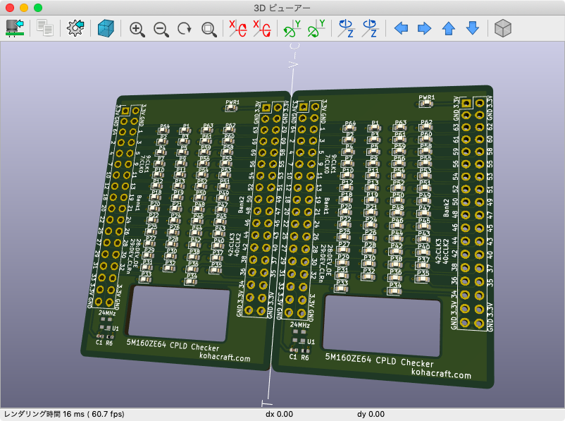
Since it is cheaper to manufacture PCB up to 10cm x 10cm, I made it about 10cm square by impositionning 4 PCB.
The top and bottom of the board have slits (holes) instead of V-cutting. A hole is needed in the top of the PCB to prevent the USB-C connector's insertion point from hitting the PCB. The components are placed at the bottom of the board, just barely to the edge of the PCB. When the board is divided, V-cuts may put stress on the parts, so slits were used instead of V-cuts.
In addition, there are 1mm holes in the four corners of the discarded PCB. This is used to align the stencil with the PCB when printing solder with the stencil. I can insert a thumbtack into this hole to ensure a perfect alignment between the PCB and the stencil.
Even if there is a hole in the data, setting is required when ordering the stencil. As shown in the figure below, it is necessary to set "Fiducials" to "Etched Through" in the stencil order setting of each PCB manufacturer.


The PCB design is complete

I have completed the design of the 5M160 stick evaluation PCB with an oscillator, making it even slimmer and easier to experiment with.
You can buy here👇👇👇
Let's see, I would like to order to PCBWay . Please refer to our previous article on how to order PCBWay.


