I want to play games with an Nintendo Famicom controller
When playing on a PC with an emulator such as NES, you will be playing with a gamepad that is sold to the general public. At this time, the Super Nintendo has a gamepad that looks like that, but
For the Nintendo Famicom, only a slightly different gamepad is available.
So, I previously converted an Nintendo Famicom controller into a gamepad using the Arduino Pro micro.
This modification method is cheaper, but the wiring is a bit troublesome. So we decided to make a special PCB for it.
FCPad's circuit
The circuit is exactly the same as the Arduino Pro micro. The idea was to put the Pro micro's circuitry inside the Nintendo Famicom controller PCB.
Artwork
Design the PCB so that it has the same shape as the Nintendo Famicom controller PCB. I printed out the design and checked if the size, holes, and pad positions were the same as the PCB.
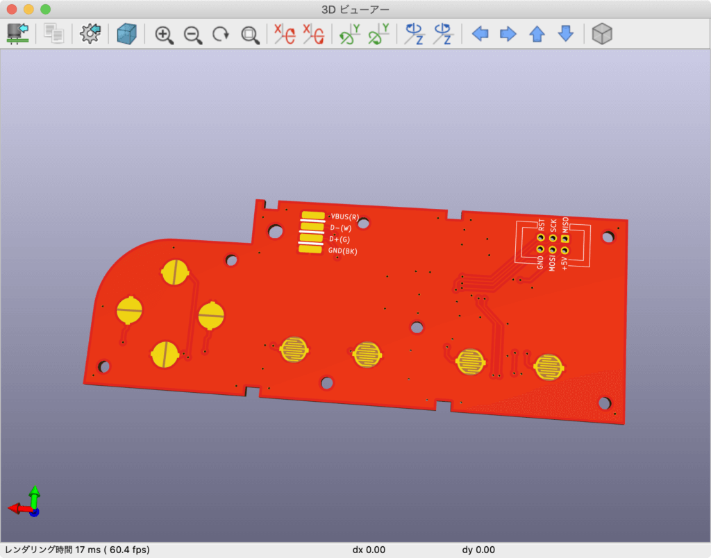
Here is the pad side. The Nintendo Famicom pad was shaped like two separate crosshairs, select, and start keys, and the AB button was shaped like a comb. The shape that splits into two is not very responsive when the buttons are pressed at an angle, but I tried to design it so that only the crosshairs are split into two, just like the real thing.
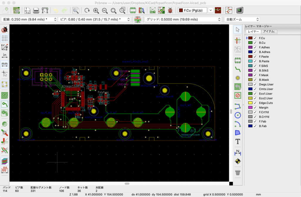
Here is the back. It contains parts for the Arduino Pro micro.
Imposition
The size of a single controller PCB is 113 mm (width) and 43 mm (height). If it imposed two, the size would be 113mm wide and 100mm long, and the price would be almost the same whether the length was 43mm or 100mm, so it imposed two.
The only regret is that the width is 113mm, which exceeds the cheaper 100mm size of the PCB, and this makes the price higher.
Order to PCBWay
I will place an order with PCBWay, who always does a good job.
Order PCBs
Click on "Quote Now" with a size of 100 length and 113 width, and a quantity of 10 sheets.
Since this is a surface-mounted board, I set "Board Type" to "Panel by Customer" and "X-out Allowance in Panel" to "Accept". X-out Allowance in Panel means that even if one of the imposition PCBs is defective, the entire PCB will be shipped as a good product. However, the PCB of the failed one will have a ❌ written on it with magic marker, so you can tell it is defective by looking at it.
The cost of the imposition PCB was the same as the non-imposition PCB. This is great because more and more PCB shops are charging extra for imposition PCBs.
The color of the board is red, and the surface treatment is electroless gold flash (ENIG) because we want it to be gold plated. The pads for the buttons are built into the PCB this time. If the surface treatment is solder plating, the contact will gradually become worse and worse, the button will stop responding. To prevent the button pads from corroding, they should be gold plated instead of solder plated, which will not corrode.
The serial number is then printed on the discarded board, rather than inside the PCB.
and wrote it in the "Other Special request" section. Usually, they print the serial number on the discarded board even if you don't write it, but there was one time when the serial number was printed on the mainboard instead of the discarded board, so I write it.
Order stencil
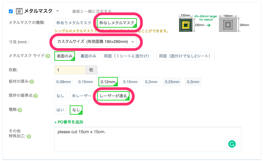
The metal mask will be fixed to the PCB with thumbtacks, as usual, so I click "Non-framework". The size is the smallest, 190mm x 290mm.
There are holes in the four corners for positioning with thumbtacks, so make sure the "Existing fiducials" is "lasered through" so that the holes can be drilled reliably.
I don't need a large stencil, so I'm going to ask PCBWay to cut it to 15cm x 15cm in the "Other Special request" section,
I wrote it down.
Uploading data and waiting for review
Once you upload your Gerber data, PCBWay staff will review it to make sure it is correct.
Soon after the review is finished, payment is made, and the order is completed.
Bug found in the PCB
I received an email from PCBWay at midnight of the day I placed the order.
Hi,
Good day.
There is an engineering question of your order W******ASF** need your check:
See attached screenshots, for the pointed areas there is small copper trace which seems will cause short circuit ?
Could you pls check and advise if we should delete the small copper trace ?
OR, just make as it is in your gerbers ?
Awaiting your prompt reply to proceed ASAP, thank you !

This was clearly a bug. By mistake, a short piece of wiring had gone into the gap between the pads. Perhaps because it wasn't a complete short, it didn't seem to cause an error in the DRC check, and I didn't notice it until you mentioned it.
I thought, "I'm glad PCBWay noticed. "Please delete it," I emailed, and the matter was settled. Thank you to the PCBWay staff, even though it was late at night.
Preview in the state of a single PCB
When I uploaded the data and completed the review, I was able to review the image when it was split into a single PCB, even though I had uploaded the imposition PCB.
The outer diameter of the board for this controller has a lot of indentations, and I was worried about whether it would cut through well, so I was glad to see this shape.
It's PCBWay professional and very useful.


