The Way to Original ROM for Famicom
I wanted to make a "My Original ROM" for Nintendo Famicom.
First, I disassembled the cassette of the Famicom as shown in the following article.
Next, I created a UV-EPROM writer as shown in the following article.
In addition, we created a UV-EPROM ultraviolet erasing device (eraser) as shown in the following article.
Famicom cassette with a socket
Now that we can erase and write to UV EP-ROM, we would like to prepare a cassette board that can be inserted into Famicom.
Substrate

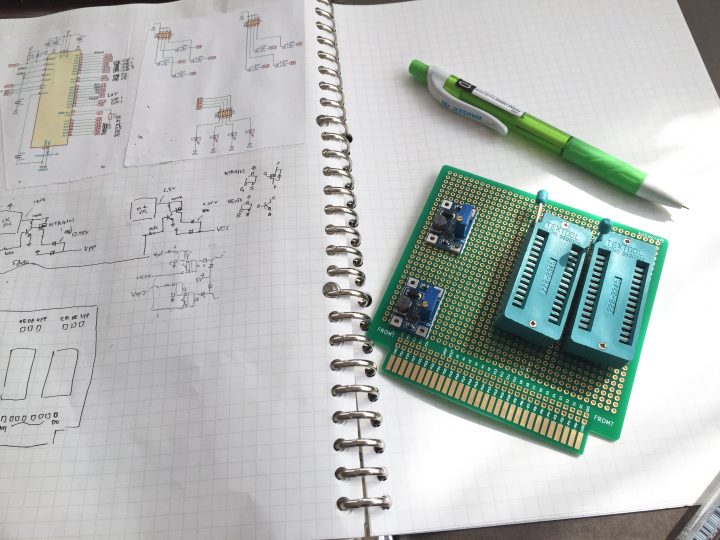
The Substrate for the Famicom cassette uses the previously made Arduino cassette board.
Cassette Arduino is an original Arduino-compatible machine with an expansion board that is a cassette for a family computer.
I made a ROM writer with this.
ZIF (Zero-Insertion-Force) Test Socket
I would like to make a mechanism that the UV EP-ROM written by the ROM writer is inserted into the socket of the cassette board.
The socket can be an ordinary IC socket, but I will change it to ZIF (Zero-Insertion-Force) Test Socket in consideration of repeated insertion and removal.
For zero-pressure sockets, when the lever is raised, the socket hole expands and the IC can be inserted.
Then, when you pull down the lever, the socket hole closes and the IC foot is locked.
ZIF (Zero-Insertion-Force) Test Socket is ideal for frequent insertion and removal because it does not cause stress to the IC leg.I need 2 pieces this time, so I bought a set of 2 pieces.
Analysis of the cassette substrate

Before, I bought several pieces of "4 person hit mah-jongg" and "baseball" and dug out a cassette board with a DIP-type ROM.
I pulled out the ROM of this board and checked the wiring.
The name of the board is "HVC-NROM - 03".

The PRG ROM had A14 wired to the 5V terminal.
The data of the program seems to start from address 4000H.
In the CHR ROM, A14 was wired to 5V and A13 was wired to GND.
It seems that the data starts from address 4000H and uses only 8 kb.
I'm not sure if it's common to start with 4000H. So, for now, I changed A14 to Hi or Low by switching it with a switch.
A10 (21 pins) and A11 (23 pins) of the CHR ROM were connected to the 18 pins of the card edge connector by jumper wire. It is written on the board that A10 is H and A11 is V.
In addition, 45 pins and 46 pins , 48 pins and 49 pins ,of the card edge connector of the board were connected.
Soldering

We soldered the parts to the cassette board of the cassette Arduino. This time, since there are only a few parts, this was finished immediately. However, the number of wires on the back side is too large.

The wiring of the power supply is made with 0.6 mm solder plated wire.
Solder-plated wire is different from tin-plated wire. Solder spreads well and it is easy to solder.
Resistance legs and capacitor legs are easy to be soldered.
It is the same as that.
The tin plated wire needs to be soldered or rubbed with sandpaper as a preliminary work.However, the solder-plated wires do not need them, and they can be wired immediately.The price is high, but the work efficiency is so high that I can't go back to the tin plated wire.
The wires are made of 0.1 mm polyurethane copper wire. The wires for signal wires and other wires that do not require electric current have a thickness of 0.1 mm, which is flexible and easy to use.
Also, if you attach the solder to the tip of the soldering iron and insert the polyurethane copper wire into the melted solder, you can melt the coating easily. If you buy 1 of them, you can use them for the rest of your life, so this is also recommended.

Now that all the wiring has been done, I have finished checking the operation by running electricity. I have attached labels to the sockets and switches to make it easier to understand.
Completion

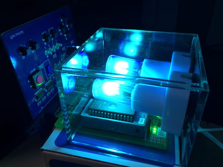
It looks like the picture above when you insert it into a Nintendo Famicom. In a normal cassette, the ROM is on the back side of the board, but the board we made this time has the ROM on the front side. It is cool to see the ROM.
Next time, I will try to burn some ROM data to UV EP-ROM and see if it works.


