This article is a contribution to PCBWay PCB Design Tutorial.
SMD Stencil
Before surface mount components can be mounted on a board, it is necessary to print solder paste on the pads of the PCB. A stencil made of thin stainless steel is used as a screen when printing solder paste.
If you don't have a stencil printer, align the pads on the board with the holes on the stencil, looking closely at the board and stencil to make sure they are aligned correctly. Then, fix the stencil with tape.
For 1.27mm pitch or 0.8mm pitch ICs, this method can be used for alignment, but for narrow pitch pads such as 0.5mm pitch or 0.4mm pitch, this alignment becomes very difficult.
Alignment using pins
Diameter measurement
So here is a simple way to align them using pins.
Measure the diameter of the pin. My pin was 0.9mm in diameter.
Creating a library
Create a library of holes for pins in KiCad's Footprint Editor.
Place one pad. Double-click it to open its properties.
- Hole size X: Pin diameter + 0.1mm
- Size X: Pin diameter + 0.1mm
- Check F.Paste
Click [Local Clearance and Setting] Tab
- Solder mask clearance: 1mm
- Click[OK]
Click [Local Clearance and Setting] Tab.
The library is now complete, with a hole of 1 mm diameter and a solder mask hole of 1 mm diameter above it.
Placed in the four corners
Place the footprints you have just made on the four corners on the breakaway rails.
Holes have been drilled in the four corners of the PCB. Let's look at the Gerber data as well.
Here is the drill data. You can see that the holes are drilled in the four corners.
Here is the Solder Mask. You can see that the stencil has a hole in it.
Ordering
You can also order stencils along with the PCB at PCBWay.
- Stencil type: Non-framework
- Existing fiducials; Lasered through
When I didn't specify "lasered through" with a different manufacturer, the stencil didn't have a hole, so I specified "lasered through" to ensure a hole.
If the size of the stencil is also large, it will be inconvenient to handle, so if the board size is 10cmx10cm, cut the stencil to 15cmx15cm to make it easier to work with.
Solder paste printing
When you receive the board and stencil, make sure that the holes are drilled in the four corners of the board.
Prepare to print solder paste.
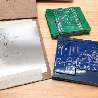
Place a piece of cardboard underneath and place a PCBs of the same thickness as the target PCB, around the target PCB.
Place the stencil on top and fix it with pins.
By sticking the pins in, the pads on the PCB and the holes in the stencil are perfectly aligned.
It is a credit card or membership card made of plastic, so it prints solder paste.
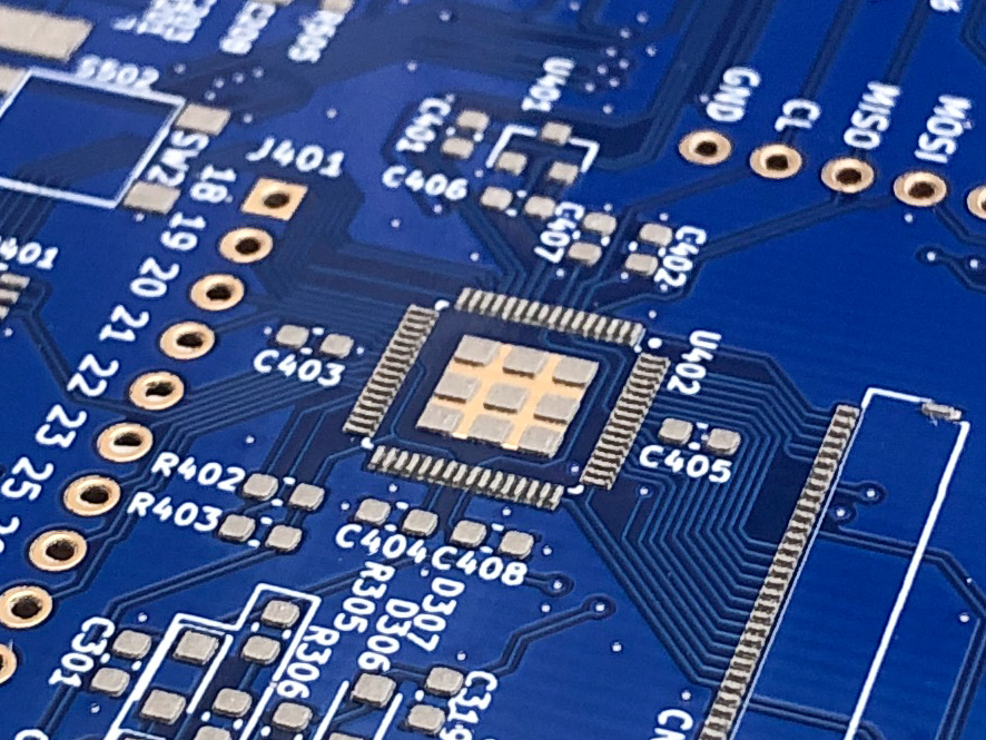
The center of the photo shows a 0.4mm pitch package with solder printed in perfect position.
Mounting and Reflow
Mount the components.
reflow it in the oven.
実装された基板の完成です。
Since the solder paste is printed in the exact position, it can be reflowed very nicely.


